You might be able to hack devices on the other side of the world or build slick web apps, but do you actually understand how your computer works? I’m not talking about what the OS does, how Java’s garbage collector behaves, or how a C++ compiler is built. I mean the lowest, hardware level—below assembly: how the hardware itself works.
- What happens inside a network interface controller when an Ethernet frame arrives?
- How is that frame transferred into the computer’s RAM over PCI Express?
- How do the fastest image recognition systems work at the hardware level?
To answer these questions, you need some grasp of the digital logic behind ASICs, but jumping straight into them is complex and expensive—it’s better to start with an FPGA.
info
FPGA stands for field-programmable gate array; in Russian they’re called “программируемые пользователем вентильные матрицы” (ППВМ). More broadly, they fall under ПЛИС — programmable logic integrated circuits.
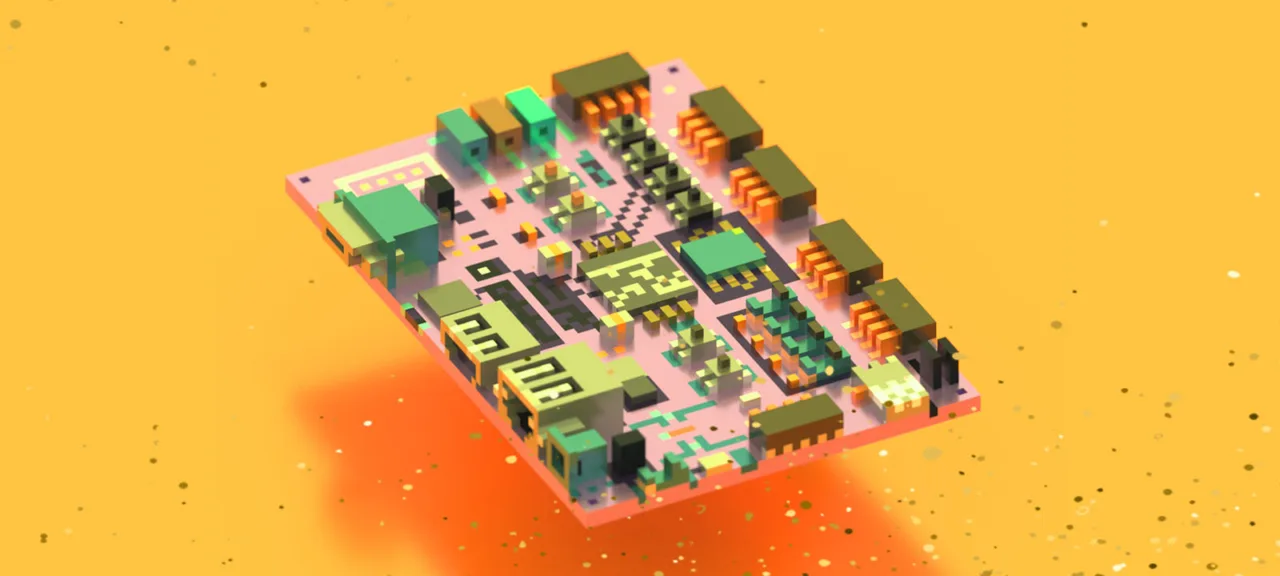
With an FPGA you can quite literally design digital chips at home, using an affordable dev board on your desk and a vendor toolchain that costs a couple of thousand dollars. There are free options as well. And it’s design, not programming: the end result is a physical digital circuit that implements an algorithm in hardware, not a program running on a CPU.
Here’s roughly how it works. You use an off-the-shelf PCB with a set of interfaces wired to an onboard FPGA—something like a high-end data center card or a training/development board.
Until the FPGA is configured, the chip has no logic to handle data from its interfaces, so nothing will work. The design process produces a bitstream that, once loaded into the FPGA, implements the digital circuitry we need. For example, you can build a 100G Ethernet controller that receives and processes network packets.
A key feature of FPGAs is their reconfigurability. Today you might need a 100G Ethernet controller; tomorrow the same board can be repurposed to implement four independent 25G Ethernet interfaces.
There are two major FPGA vendors: Xilinx and Intel, holding 58% and 42% of the market, respectively. Xilinx’s founders created the first FPGA back in 1985. Intel entered the market more recently—in 2015—by acquiring Altera, which was founded around the same time as Xilinx. Xilinx and Altera’s technologies are largely similar, as are their development environments. I’ve worked more with Xilinx products, so don’t be surprised by the frequent references to it.
FPGAs are widely used in a range of devices: consumer electronics, telecom equipment, accelerator cards for data centers, robotics, and for prototyping ASICs. I’ll cover a couple of examples below.
We’ll also look at the technology that enables hardware reconfiguration, walk through the design flow, and go over a simple example of implementing a hardware counter in Verilog. If you have any FPGA development board, you’ll be able to follow along on real hardware. If you don’t, you can still get familiar with Verilog by simulating the circuit on your computer.
How it works
An FPGA is, like an ASIC, a custom silicon device built from the same transistors used to implement flip-flops, registers, multiplexers, and other logic for conventional circuits. You can’t, of course, change how those transistors are physically wired. But the chip’s architecture is designed so that you can reconfigure the interconnect between larger functional blocks, known as CLBs—configurable logic blocks.
You can also change the logic function a CLB implements. This is possible because the entire chip is crisscrossed with configuration memory cells (SRAM). Each bit of that memory either controls a signal-routing switch or serves as part of the truth table for the logic function implemented by the CLB.
Because the configuration memory is based on SRAM, first, the FPGA must be configured at power-up; second, the device can be reconfigured virtually unlimited times.

CLB blocks are embedded in a switching matrix that determines how the inputs and outputs of the CLBs are interconnected.

At each conductor intersection there are six switching transistors, each controlled by its own configuration memory cell. By turning some on and others off, you can route signals between CLBs in different ways.

Very roughly, a CLB consists of a block that implements a Boolean function of several inputs (a Look-Up Table, or LUT) and a flip-flop (FF). In modern FPGAs, a LUT typically has six inputs, but the figure shows three for simplicity. The LUT’s output can be sent to the CLB output either asynchronously (directly) or synchronously (through the FF, which is clocked by the system clock).

It’s instructive to look at how a LUT is implemented. Take the Boolean function y . Its schematic representation and truth table are shown in the figure. The function has three inputs, so it yields 2^3 = 8 output values, each corresponding to a specific input combination. These values are computed by the FPGA design tools and stored in dedicated configuration memory cells.
Each LUT entry’s value is routed to a dedicated input of the LUT’s output multiplexer, and the Boolean function’s input arguments select which value is output. The CLB is one of the key hardware resources in an FPGA. The number of CLBs in modern FPGA dies varies by device type and capacity. Xilinx offers devices ranging from roughly four thousand to three million CLBs.
Beyond CLBs, FPGAs include other important hard resources—for example, multiply–accumulate units, often called DSP blocks. Each can perform 18-bit multiply-add operations every clock cycle. In high-end devices, the number of DSP blocks can exceed 6,000.
Another key resource is on-chip memory blocks (Block RAM, BRAM). Each block holds 2 KB. Depending on the device, total BRAM capacity can range from 20 KB up to 20 MB. Like CLBs, BRAM and DSP blocks are tied into the routing fabric and are distributed across the entire die. By interconnecting CLB, DSP, and BRAM blocks, you can build highly efficient data-processing architectures.
FPGA Applications and Advantages
Xilinx’s first FPGA, introduced in 1985, had only 64 CLBs. At the time, transistor density on ICs was far lower than it is today, and digital systems often relied on discrete logic chips. There were separate chips for registers, counters, multiplexers, and multipliers. Each device had its own custom PCB populated with these low-integration ICs.
Using an FPGA made it possible to abandon that approach. Even a small FPGA with 64 CLBs (configurable logic blocks) saves significant board space, and reconfigurability adds the ability to update device functionality after manufacturing, during operation—in the field—hence the name “field‑programmable gate array.”
Because an FPGA can be configured to implement virtually any digital hardware circuit—as long as there are enough resources—one of its key uses is prototyping ASICs.
ASIC development is highly complex and costly; the price of a mistake is very high, and logic verification is critical. Therefore, before starting the chip’s physical design, one of the development stages was to prototype the design on one or more FPGA devices.
For ASIC development, engineers use special boards that incorporate many interconnected FPGAs, such as these specialized boards. The prototype chip runs at much lower clock rates—often only tens of megahertz—but it helps uncover issues and bugs early, saving time and money.
However, I think FPGAs have even more compelling use cases. Their flexible fabric lets you build hardware circuits for high-throughput, highly parallel data processing, while keeping the algorithm reconfigurable.

Let’s think about how CPUs, GPUs, FPGAs, and ASICs differ at a fundamental level. A CPU is general-purpose: you can run virtually any algorithm on it. It’s the most flexible and the easiest to use thanks to the vast ecosystem of programming languages and development tools.
At the same time, the CPU’s general-purpose nature and sequential instruction execution reduce performance and increase the system’s power consumption. That’s because for every useful arithmetic operation, the CPU has to do a lot of extra work: fetching instructions, moving data between registers and the cache, and other overhead.
On the other end is the ASIC. On this platform, the required algorithm is implemented directly in hardware by wiring transistors; every operation is dedicated to that algorithm, and there’s no way to change it. This yields maximum performance and the lowest power consumption. The downside: you can’t reprogram an ASIC.
To the right of the CPU is the GPU. These chips were originally designed for graphics processing, but are now also used for mining general-purpose computing. They consist of thousands of small processing cores and execute parallel operations on arrays of data.
If an algorithm can be parallelized, a GPU can deliver significant speedups over a CPU. On the other hand, sequential algorithms tend to perform worse, making the platform less flexible than a CPU. Developing for GPUs also requires specialized skills and familiarity with OpenCL or CUDA.
Finally, FPGAs. This platform combines ASIC-like efficiency with the ability to reprogram. FPGAs aren’t general-purpose, but there’s a class of algorithms and workloads where they outperform CPUs and even GPUs. Developing for FPGAs is harder, but newer toolchains are narrowing that gap.
The decisive advantage of FPGAs is their ability to process data as it arrives, with minimal latency. For example, imagine an intelligent network router with many ports: when an Ethernet packet hits one of its ports, it has to evaluate a large set of rules before selecting the egress port. It may also need to rewrite certain packet fields or add new ones.
Using an FPGA lets you handle this on the fly: as the first bytes of a packet start arriving from the network interface, its header is already being analyzed. Relying on CPUs here can significantly reduce packet processing throughput. Sure, you could build a custom ASIC for routers to achieve maximum efficiency, but what if the packet-processing rules need to change? Only an FPGA can deliver the required flexibility while maintaining high performance.
Therefore, FPGAs are used in scenarios that demand high data-processing performance, minimal response time, and low power consumption.
FPGA in the cloud
In cloud computing, FPGAs are used for fast computation, accelerating network traffic, and rapid access to large datasets. They’re also widely adopted for high-frequency trading on financial exchanges. Servers typically host FPGA boards with PCI Express and optical network interfaces from Intel (Altera) or Xilinx.
FPGAs are a great fit for cryptographic algorithms, DNA sequence alignment, and scientific workloads like molecular dynamics. Microsoft has long used FPGAs to accelerate the Bing search service, and to build software-defined networking inside the Azure cloud.
The machine learning boom hasn’t left FPGAs behind. Companies like Xilinx and Intel offer FPGA-based solutions for deep neural networks. These tools can generate FPGA bitstreams that implement a given network directly from frameworks such as Caffe and TensorFlow.
You can even try all of this from home using cloud services. For example, on Amazon you can rent a virtual machine with access to an FPGA board and a full set of development tools, including machine learning.
FPGA on the edge
What else do people build with FPGAs? Practically everything—robotics, autonomous vehicles, drones, scientific instruments, medical devices, consumer mobile gadgets, smart surveillance cameras, and more.
Traditionally, FPGAs were used for one-dimensional digital signal processing (competing with DSP processors) in radar systems and RF transceivers. As chip integration and platform performance have improved, FPGAs have been increasingly adopted for high-performance computing—for example, for two-dimensional signal processing at the edge (edge computing).
This concept is easiest to understand with the example of a traffic camera that performs license plate recognition. You can use a camera that streams video over Ethernet and process the feed on a remote server. As the number of cameras grows, the network load will increase, which can lead to system instability or failures.
Instead, it’s better to run license plate recognition on a compute unit built directly into the camera housing and send only the plate numbers to the cloud as text. You can even use relatively inexpensive, low-power FPGAs so the system can run on a battery. This also keeps the option to update the FPGA’s logic—for example, if the license plate standard changes.
When it comes to robotics and drones, two requirements are especially critical: high performance and low power consumption. FPGA platforms are a great fit and can be used, for example, to build flight controllers for drones. There are already UAVs capable of making decisions on the fly.
How do you design an FPGA project?
There are several design levels: low, block-level, and high. The low level uses languages like Verilog or VHDL, where you work at the register-transfer level (RTL). Here, you define registers (as in a CPU) and the logic that transforms data as it moves between them.
FPGA designs run at fixed clock rates (typically 100–300 MHz), and at the RTL level you define the circuit’s behavior on a per-clock-cycle basis. This meticulous work yields highly optimized designs in terms of performance, FPGA fabric/resource utilization, and power consumption. But it requires serious digital design skills, and even then the process isn’t fast.
At the block level, you’re mostly integrating prebuilt, high-level blocks that implement specific functions to achieve the desired functionality of a system-on-chip (SoC).
At a higher level of design, you’re no longer managing data on every clock cycle; instead, you focus on the algorithm. There are tools that compile C and C++ into RTL, such as Vivado HLS. It’s quite capable and can synthesize a wide range of algorithms into hardware.
The key advantage of this approach over RTL languages is speed—especially for development and testing. You can run and verify the C++ implementation on a computer, which is far faster than testing algorithm changes at the RTL level. The trade-off is that convenience comes at a cost: the resulting hardware may be slower and consume more resources.
We’re often willing to pay that price: if you use the compiler wisely, performance won’t suffer much, and modern FPGAs have resources to spare. In our world, where time to market is critical, that trade-off is justified.
Often a single design has to combine all three development styles. Suppose we need to build a device we can embed in a robot and give it the ability to recognize objects in a video stream—for example, road signs. We’ll take an image sensor chip and wire it directly to the FPGA. For debugging, we can use an HDMI monitor connected to the FPGA as well.
Frames from the camera will be fed into the FPGA over an interface defined by the image sensor vendor (USB isn’t an option here), then processed and sent to a monitor. You’ll need a framebuffer for this, which typically resides in external DDR memory mounted on the PCB next to the FPGA chip.

If the image sensor vendor doesn’t provide an interface IP core for our FPGA, we’ll have to implement it ourselves in RTL, handling timing, bits, and bytes according to the data transfer protocol specification. We’ll likely use off‑the‑shelf Preprocess, DDR Controller, and HDMI IP blocks and simply hook up their interfaces. And the HLS block that performs detection and processing on the incoming data can be written in C++ and synthesized with Vivado HLS.
Most likely we’ll also need an off‑the‑shelf traffic sign detection and classification library adapted for FPGA use. In this example I’m showing a heavily simplified block diagram of the design, but it accurately reflects the operational logic.
Let’s walk through the design flow—from writing RTL code to generating the configuration bitstream for loading into an FPGA.

You’re writing RTL code to implement the design you need. Before trying it on real hardware, you should verify that it’s correct and meets the requirements. To do that, run RTL simulations on your computer using a simulator.
You take your design—currently only in RTL code—drop it onto a virtual testbench, drive sequences of digital signals into the inputs, capture the output waveforms and their timing, and compare them against the expected results. Usually you uncover bugs and go back to refining the RTL.
Next, the logically verified code is fed into the synthesis tool. It converts the textual description of the design into a netlist of digital primitives from the library available for the target FPGA. This netlist includes elements such as LUTs, flip-flops, and the connections between them. At this stage, the elements are not yet bound to specific hardware resources. To do that, you must apply design constraints—for example, mapping your design’s logical inputs and outputs to the FPGA’s physical I/O pins.
These constraints also require you to specify the clock frequencies the design must run at. The synthesizer’s output and the constraints file are then handed off to the Implementation stage, which, among other tasks, performs placement and routing (Place & Route).
During Place, each still-unassigned element from the netlist is mapped to a specific resource on the FPGA. Next, Route kicks in, attempting to find the optimal connections between these elements using the device’s switch matrix (routing fabric).
Place and Route work from the constraints we set on the design: I/O pin assignments and clock frequency. The clock period has a major impact on implementation: it must not be shorter than the propagation delay through the logic on the critical path between two successive flip-flops.
Often you can’t meet this requirement right away, so you have to go back to the initial stage and modify the RTL—for example, by reducing the logic on the critical path. After Implementation completes successfully, we know where each element is placed and how they’re connected.
Only after that do you generate the FPGA bitstream. The next step is to load it onto real hardware and verify that it behaves as expected. If problems arise at this stage, it means the simulation was incomplete and didn’t catch all the bugs and issues.
You can roll back to the simulation stage and model the abnormal scenario; if that still doesn’t help, there’s a last‑resort on‑chip debug mechanism that works on the live hardware. You specify which signals to trace over time, and the development environment generates an additional logic analyzer core that’s placed on the die alongside your design, taps into the signals of interest, and records their values over time. The captured waveforms can then be exported to a computer for analysis.
There are high-level design tools (HLS, high-level synthesis) and even ready-made frameworks for building neural networks on FPGAs. These tools generate RTL code in VHDL or Verilog, which then goes through the toolchain: Synthesis → Implementation → Bitstream generation. They’re perfectly usable, but to use them effectively you still need at least a basic understanding of RTL-level languages.
To be continued
I hope the theory didn’t overload you too much! In the next article, I’ll get into the hands-on part: we’ll look at exactly what you need to do to program an FPGA.