
So you’ve got that flashy new high-tech gadget. It could be a smart home controller or a top-notch interactive media streaming box – the one that can tune in to thousands of channels from all over the world and make an espresso during commercial breaks. But how to find out what this gadget is doing behind your back?
Who can guarantee that the media streaming box connected to our Wi-Fi network does not covertly collect passwords to your favorite websites, while the smart home setup does not stream videos from our bedroom via security cameras? (They do, from time to time). To protect ourselves from such a ‘rise of the machines’, one must understand how the gadget works, and secure it against intrusions.
There aren’t that many publications about smart device security. Today is the day we’re going to fix it.
Smart Device Security
Since 2018, the Internet of Things security issues have been broadly discussed in connection with malware attacks (e.g. Mirai and VPNFilter) affecting home gadgets. To protect ourselves against such troubles, you have to have a good understanding of the hardware and operation principles of smart gadgets. In other words, you must know how to test them in a right way.
The Internet of Things testing can be broken into four stages:
- intelligence: reviewing information on the gadget in public sources to discover supported protocols, compatible devices, servers it connects with, etc.;
- hardware research: examining the device’s mainboard;
- software research: dumping and examining its firmware; and
- testing its network and wireless communications.
In this article, we are going to address hardware security issues and learn how to disassemble a device to examine its debug interfaces.
Our primary objective is to extract the gadget’s firmware or get access to its management console. In case you are a novice in this sphere, the article provides a detailed step-by-step walkthrough to successfully accomplish this task.
Why is it so important to research the mainboard of the device? There are three types of security analysis: ‘black box’ testing (no information on the system is available), ‘gray box’ testing (some implementation features of the system are known), and ‘white box’ testing (we know all peculiarities of the tested system).
The ‘lighter’ is the box, the higher is the security analysis efficiency. Therefore, in the course of the testing, we must collect as much data as possible to advance from lower testing levels to the higher ones.
Here is an example. When you first meet the device, you know nothing about it. Therefore, ‘black box’ testing must be applied.
So you’ve got it disassembled and managed to extract its debugging log via debug ports. The testing automatically becomes easier and advances to the ‘gray box’ level. Then you find the root password in debug logs, and then you use it to connect to the management console. Then you have access to the file system. At this stage, the testing advances to the highest ‘white box’ level.
Disassembling the device
Most probably, some readers are going to skip this section. A few months ago, I would do so, too; however, it turned out that the topic includes plenty of subtle nuances, and their knowledge makes the life of a novice researcher much easier.
Screws
To make the job of device crackers as difficult as possible, OEMs invented plenty of special weirdly-shaped screws.

This is done on purpose: if you cannot undo the screws and have to use other methods to open it, chances are high that either the body or the fragile mainboard are damaged, and your warranty goes the way of the dodo. The picture below shows a classic example of such a screw.

Here is the Apple’s security screw concept.

To be prepared to such surprises, you will need a good set of screwdrivers with all required tips. I am not going to advertise specific brands (they don’t pay Hacker for that, or I definitely would), but the average price of a special toolkit designed for disassembling mobile devices can be around $60.

Still, even the most advanced screwdriver kit do not guaranty a 100% success. I encountered devices with regular screws, but when I was unscrewing them, plastic parts with internal screw threads inside the case were breaking off. Therefore, a great caution must be exercised when dealing with fragile devices. Screwdrivers require skillful hands!
Protection from cracking: foreign materials on the mainboard
I guess you had already disassembled electronic devices out of curiosity when you were a child, and examined mainboards of various gadgets. Often, a strange black ‘blot’ can be found on them like the one shown below.

This is a compound consisting of solidified polymer resin with certain additions. It is used as an electric insulating material; sometimes it also prevents the connection to certain contacts on the mainboard. The most popular compound base is epoxide resin.
The Internet offers numerous tips on removing it in various situations. I suggest the most time-tested method: heat the upper layers of the resin and remove them. This technique is not as fancy as dissolution, but it works in most cases. (Guess what happens to your warranty when you do that!)
It is also necessary to note that transparent glue is sometimes used on mainboards made in China. It is easy to remove, and we won’t spend time on it.
Protection from cracking: other scenarios
In reality, other protection techniques are used very rarely. The specialist literature talks about “fuses”; after you ‘blow’ such a fuse, the device is kaput. This protection trick is very exotic; I personally don’t know of a single example of such a device. If you had encountered something like this, please share your experience in the comments.
Examining the mainboard
So, the device is cracked, and the only interesting component inside is its mainboard.
Searching Internet for info
The mainboard name or index are often printed right on top; using this information, you may find online its scheme with descriptions of all interfaces, thus skipping several testing phases that are normally carried out to identify the communication protocols.

Researching chips
In addition to the mainboard name, make sure to find and write down the names of all the chips installed. Then you can search Google for their purposes and supported interfaces.
The picture below shows a datasheet for the STM32F207 microcontroller found online; it provides detailed descriptions of all its contacts.

Examining sockets
If any sockets can be seen on the mainboard, most probably, the developers have put them there for a reason. It is also necessary to keep in mind that some ports on the device may be used for debugging.
For example, the Ethernet socket of many video cameras supports the Power Over Ethernet (PoE) mode. If this is the case, I recommend purchasing special splitters.

In addition, some devices use this port as RS-232 (I am going to address it in more detail later). If so, you will need another special cable.

Important: even if there is a suitable socket on the mainboard, no one can guarantee that the adapter will fit because there are several different pinout standards.
USB sockets are rare birds on smart devices’ mainboards; in most cases, they are used for connecting to data storage devices. Sometimes, this port may be used for debugging, such as on Android smartphones.
RS-232 ports are typically found on industrial devices; they are used for administrative purposes, and adapters to such sockets are available in stores.

Microcircuit contacts
To start working with hardware interfaces, it is necessary to identify their presence and location on the microcircuit. We are going to address the eight most common variants of their placement.
Look closely at the mainboard below.

Do you see these contacts?

I bet that some of them are intended for device debugging and support a certain interface or even a few ones. To connect to these pins, a soldering iron is required.
On some devices, such contacts may be concealed.
Here is another example. Look at the picture.

Some contacts have the form of via openings with metallic coating. You can use standard pins (e.g. for Arduino UNO) to connect to them. It is also important to watch the pin length; otherwise, the mainboard may be damaged during the connection.
Next example.

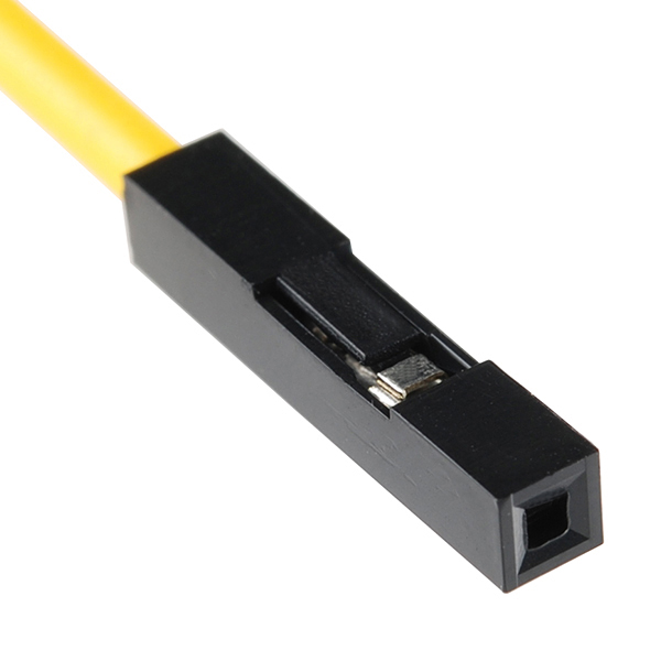
If Arduino pins do not fit, you may use another method. Take a cable with the socket shown on the next picture. Such sockets are often used to connect indicators and buttons to the computer motherboard. Remove the plastic case, then adjust the clamp size using pliers, and wrap insulating tape around it to prevent contact with adjacent pins.
This is how it was
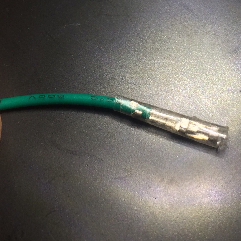
This is how it is now
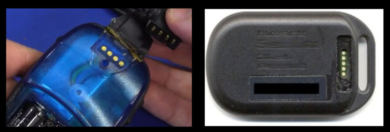
For connection convenience, the device shown on the next picture has a separate debug slot. In this case, the best solution is to connect all required contacts to separate wires using a soldering iron.
One more example.

Multilayer printed boards often have sections indicating that some unnecessary details were removed. In this particular case, chances are high that debug pins were located on a separate card removed in the course of production. I am not going to review such cases in detail; it is necessary to note however that the possibility to connect to such contacts depends on the mainboard architecture: other elements may be damaged during a connection attempt.

If you have found online a pinout scheme for the chip, you may connect to it directly as shown on the picture above. This requires good soldering skills.
Some pins may be hidden beneath a sealing layer; see the next picture. However, such things are pretty rare.

Cybersecurity researcher Dennis Giese made a presentation at DEFCON 26 about the physical protection of Xiaomi’s devices. Examining the mainboard of a gadget produced by this company, he found that the connection pad of the chips was located exactly beneath them; so, it was impossible to connect to the pins without soldering.

However, later he noticed conductive tracks leading to another chip. After that, Dennis was able to find online a datasheet for this microcircuit.

Upon reviewing the datasheet, the researcher established that these conductive tracks were MMC data lines connecting the chip with RAM. He connected to them and dumped the firmware.

Identifying contact interfaces
After dealing with the contacts, it is necessary to identify protocols supported by debug pins. In this section, let’s discuss equipment used to research communication protocols compatible with your device.
Oscillograph
You may be familiar with oscillographs. These devices allow to measure the activity on respective pins, both visually and using software tools. The main disadvantage of oscillographs is their high cost. On the other hand, you get fully-featured equipment for interface identification. In addition, many expensive oscillographs support the logical analyzer function.

Logical analyzer
There are several competing logical analyzer brands, for instance, DSLogic and Saleae Logic. The comparative characteristics of these devices are available online; in this article, I will use Saleae Logic.

Its price starts from $500 (a 50% discount is available for students). Connect the logical analyzer’s probes to the studied pins, turn the sampling mode on, and see a picture like the one shown below.

The protocols used by the selected pins can be either identified visually or by using software tools; for that purpose, the analyzer’s application interface has a special tab: Analyzers. In some cases, you have to set some parameters, for instance, the baud rate.
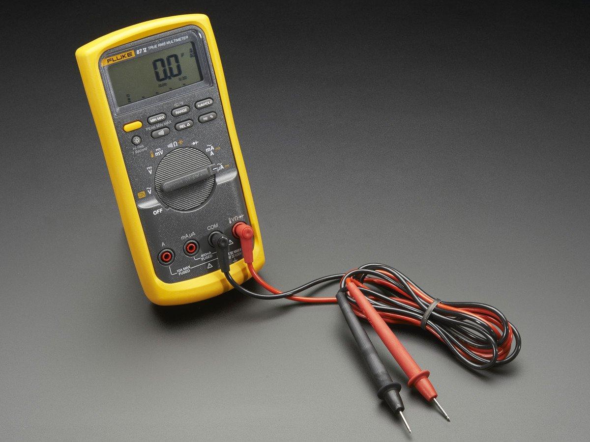
Multimeter
A multimeter allows detecting a signal on certain pins. All you have to do is find contacts where the voltage is jumping on a regular basis. This method is convenient when the studied mainboard has numerous pins and their examination using other techniques may take a good deal of time.
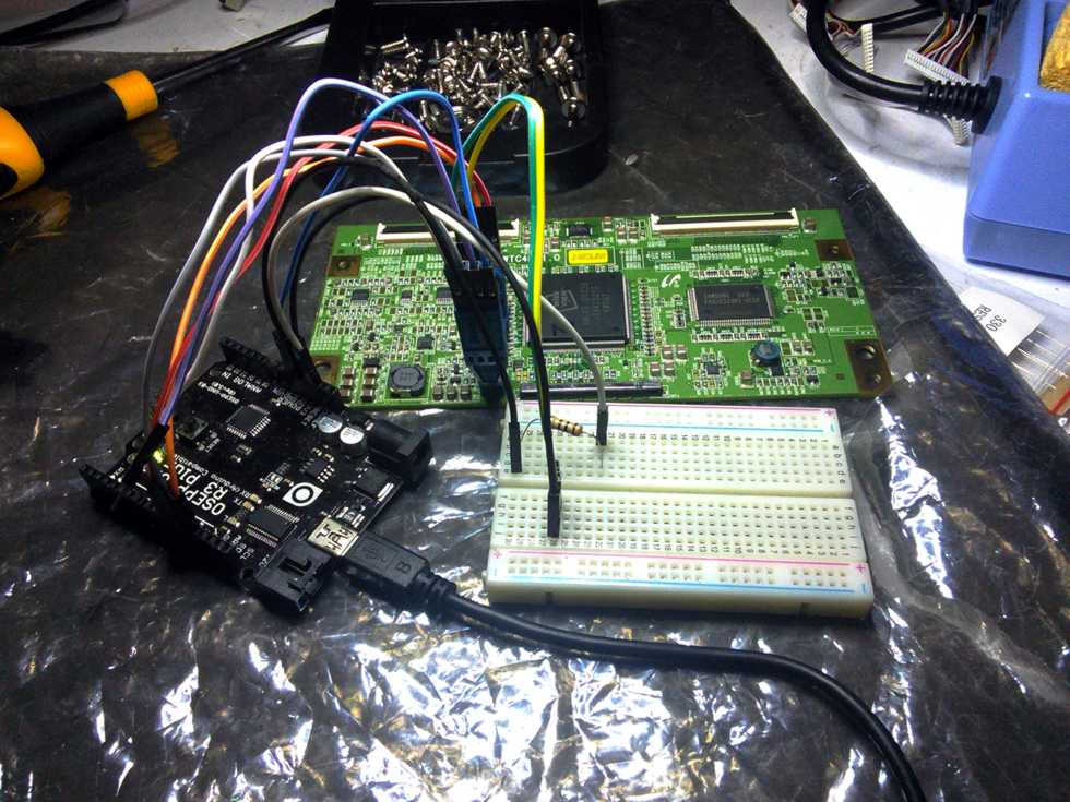
Arduino
If you have an Arduino board and a small attached screen, you can assemble a portable oscillograph. Almighty Google offers plenty of technical solutions for such devices.

JTAGenum
In some cases, you have to find out what protocol is most probably used by one or another interface. A special project entitled JTAGenum has been developed for the JTAG interface.
Using JTAGenum, the researcher may determine what pin on the mainboard is responsible for what. All you have to do is purchase an Arduino, install JTAGenum software on it, connect probes 2 to 11 to the tested mainboard, and run the scan. The next picture shows an example of its work.

JTAGulator

This glamorous pink card a la Hello Kitty performs the same functions as JTAGenum. Its benefits are as follows:
- connect up to 24 pins at a time;
- use it as a JTAG adapter;
- use it as an UART adapter; and
- an extra bonus: UART baud rate calculation.
Furthermore, researchers are currently developing software making it possible to use JTAGulator as a logical analyzer.
The only drawback is the high cost of this card, some $175.
Which card is better? See article JTAGulator vs. JTAGenum, Tools for Identifying JTAG Pins in IoT Devices for more detail (spoiler alert: both Arduino and JTAGulator have shown great efficiency and performance).
Interaction with interfaces
UART
UART is one of the most common debugging protocols. Depending on the device’s mainboard and firmware, it allows to communicate with the operating system boot loader and terminal.
The protocol uses at least two mandatory pins: RX (receiver) and TX (transmitter). The two optional pins are GND (ground) and VCC (voltage). In most cases, you have to look for four grouped pins on the mainboard.
To use an UART serial console, you will need special software; minicom is optimal for Unix-based systems, while Realterm is for Windows.
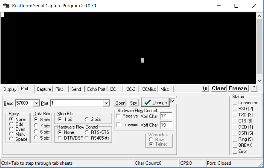
Realterm interface
After loading the program, you have to manually connect RX pins; if this does not work, then connect GND as well. A periodically interrupted (this is important!) stream of bytes should appear on the screen. Then you have to select the baud rate to make the unreadable symbols on the screen readable. The most popular rates (i.e. frequencies) are provided in the table below (the first column).

You can select the baud rate either manually (by switching between frequencies in the program) or using a popular script included in baudrate.py Python package.
Equipment
Specials adapters are required to work with UART protocol; for instance, the USB-compatible ones.

An USB to COM port adapter can also be used as an USB to UART adapter; you will only need its RD, TD, and Ground pins.
Below is an UART adapter made from an USB to RS-232 adapter.

In addition, you can use an Arduino Uno microcontroller board as an USB to UART adapter. To do so, short the Reset and GND pins together.

As an alternative, you can buy a Bus Pirate board able to fulfill a broad spectrum of tasks. In this particular case, I’ll use it as an USB to TTL adapter.

To switch the board to the adapter mode, you have to connect it to a PC and start working in the command prompt of the device on the frequency of 115 200 using the Realterm/minicom program (see above).

The tuning of this device is probably not worth a detailed description. The command listing in the course of its switching to the adapter mode is shown below.

Then you have to connect the pins as follows: MOSI → RX, MISO → TX, GND → GND, and Bus Pirate can be used as a standard adapter.
Now it is time to talk about JTAGulator again. Even though it was designed for different purposes, JTAGulator can be used inter alia as an USB-TTL adapter. Similarly with Bus Pirate, it is necessary to launch its control console and enter the commands shown below:

WARNING
Before you go wild and start experimenting, check all pins with a multimeter to make sure there is no high voltage on them. Otherwise, you may burn out devices such as Arduino and USB to UART. Surprisingly, but in my experience, USB to Serial adapters have shown the best results and never burned out during the testing.
JTAG
JTAG is the name of the workgroup that has developed IEEE 1449 standard, but many people associate it with a debugging interface. In most cases, the access to this interface grants you the unlimited control over the device, including the possibility to dump its firmware. Normally, OpenOCD on-chip debugging tool is used for communication with JTAG.
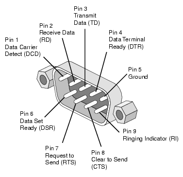
The interface includes four mandatory working pins: TDI (data input signal), TDO (data output signal), TCK (clock rate), and TMS (testing mode selection). There is also one optional pin: TRST (TestReset).

Normally, contacts on the mainboard are grouped in one or two lines; therefore, searching for the required pins may be complicated. The techniques allowing to find out what each port is responsible for have been addressed above; below are examples of communication with devices supporting JTAG interface.
Equipment
Arduino can be used as a programming tool for some chips. There are tons of projects for this device; so, if you need a programmer for a certain architecture, just search online. Most probably, somebody has already implemented it.
If we know the purpose of each pin and have a JTAGulator card, it can be switched to the OpenOCD compatibility mode and used as an adapter.
J-Link is a cheap and multifunctional programmer allowing to work with many different processors and compatible with OpenOCD; it price is about $75.


Finally, it is possible to work with the JTAG interface using a Bus Pirate board and OpenOCD software. A detailed device setup guide can be found in article Gonemad’s Bus Pirate/OpenOCD Walk Through.
I2C
This interface is mostly used for communication with EEPROM memory. At least two data lines are required for the connection. The communication monitoring techniques are described below.
Equipment
I2C activity can be monitored using Arduino – a respective project is available on GitHub.
Of course, this hardware is not sufficient to make a fully featured firmware dump, but at least it allows to make sure that data are transmitted using I2C interface. In addition, Bus Pirate may be used for working with I2C. Remember that noise may be generated during the data transmission; therefore, the obtained information is not 100% trustworthy. The pins should be connected as follows: MOSI → SDA, CLK → SCL.
A detailed tutorial on the Bus Pirate use can be found in Digitalpeer Blog.
There is also a device called I2CDriver; it connects your PC to I2C interface using an USB channel. I2Cdriver allows to not only control the gadget but to also monitor and decode its traffic. I had not used it yet, but this adapter looks very promising.

SPI
Although this interface is not used very often, it still has to be mentioned.
The Serial Peripheral Interface (SPI) is a communication interface used for serial data exchange between microcircuits. It is based on the Master-Slave principle and uses four signals: MOSI (data output from master), MISO (data output from slave), SCLK (serial clock), and CS (slave select).
Equipment
As usual, I’ll start with Arduino. A project entitled spi-dump allows using this device for firmware dumping with SPI EEPROM. I am not going to discuss it in detail; a good tutorial on this technology written by its author is available on GitHub.
Bus Pirate also supports the SPI sniffer function; its setup is similar to the one used for I2C.

The pin connection scheme is as follows: MOSI → MOSI, CLK → CLOCK, MISO → MISO, CS → CS.
SWD
I must admit I had never encountered this interface in IoT devices. However, developers of microcontrollers broadly use it, and SWD may appear in smart devices pretty soon. The interface uses the same protocol as JTAG. It requires only three pins: DIO (input-output), CLK, and GND.
Equipment
Bus Pirate does not fully support SWD; you can only write the firmware to the chip’s flash memory. The pin connection scheme is as follows: MOSI → DIO, CLK → CLK, and GND → GND.
Now that you have learned how to work with interfaces, let’s see how can this be applied to the smart device testing.
Payload
Using the above interfaces, try collecting comprehensive information about the device: the software version, source code, access to the control console, etc.
Dumping firmware…
…using UART interface
In most cases, UART can be used to communicate with the operating system bootloader . The capabilities of the bootloader’s command line interface are limited by the requirements of the mainboard developers; therefore, all possible scenarios are just too many to review. There are two sample cases with different boot loaders: Universal Boot Loader (U-Boot) and Common Firmware Environment (CFE).
To connect to the respective device’s bootloader, use one of the serial communication programs, minicom or Realterm. The baud rate has been already determined at earlier stages of this research. To activate the console, you may need to press Ctrl + C or other key combinations; therefore, it is necessary to watch messages appearing on the screen.
If you use U-Boot, you may type magic word help after connecting to the console to see the list of available commands.

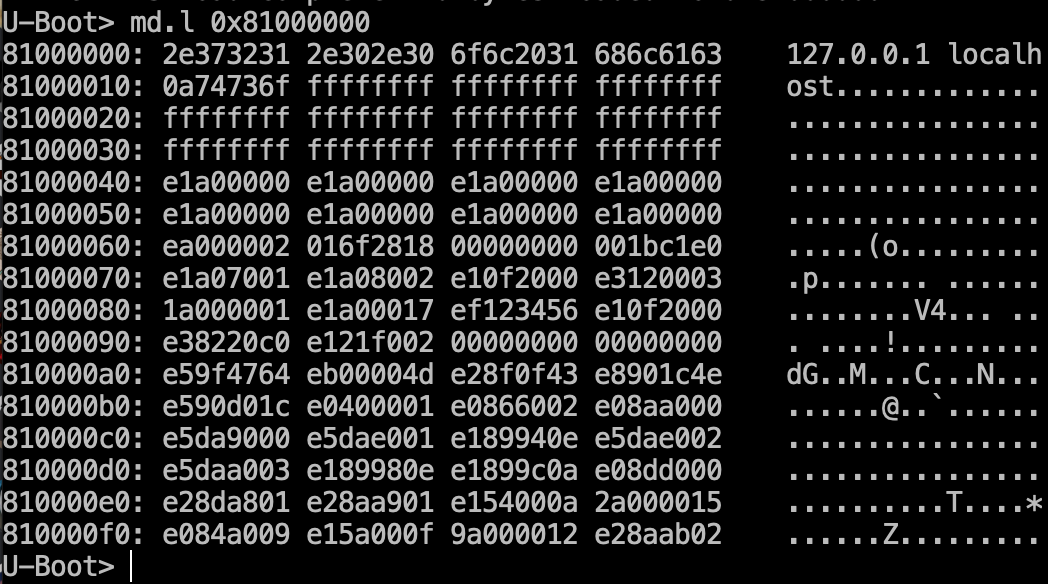
In this particular case, you’ll need three commands: cramfsls, cramfsload, and md. Using cramfsls, you can get the list of files in the file system of the device.

Then select the required file (for instance, /etc/hosts) and read it using cramfsload.

In response, there’s a message that the file is loaded to address 0x81000000 in the flash memory. We’ll read it using the md.l (memory display) command.
Over time, this process can be automated using, for instance, the PySerial library.
If you use the CFE boot loader, the only difference is the sequence of entered commands.
First, let’s see the list of connected devices using the show devicescommand.
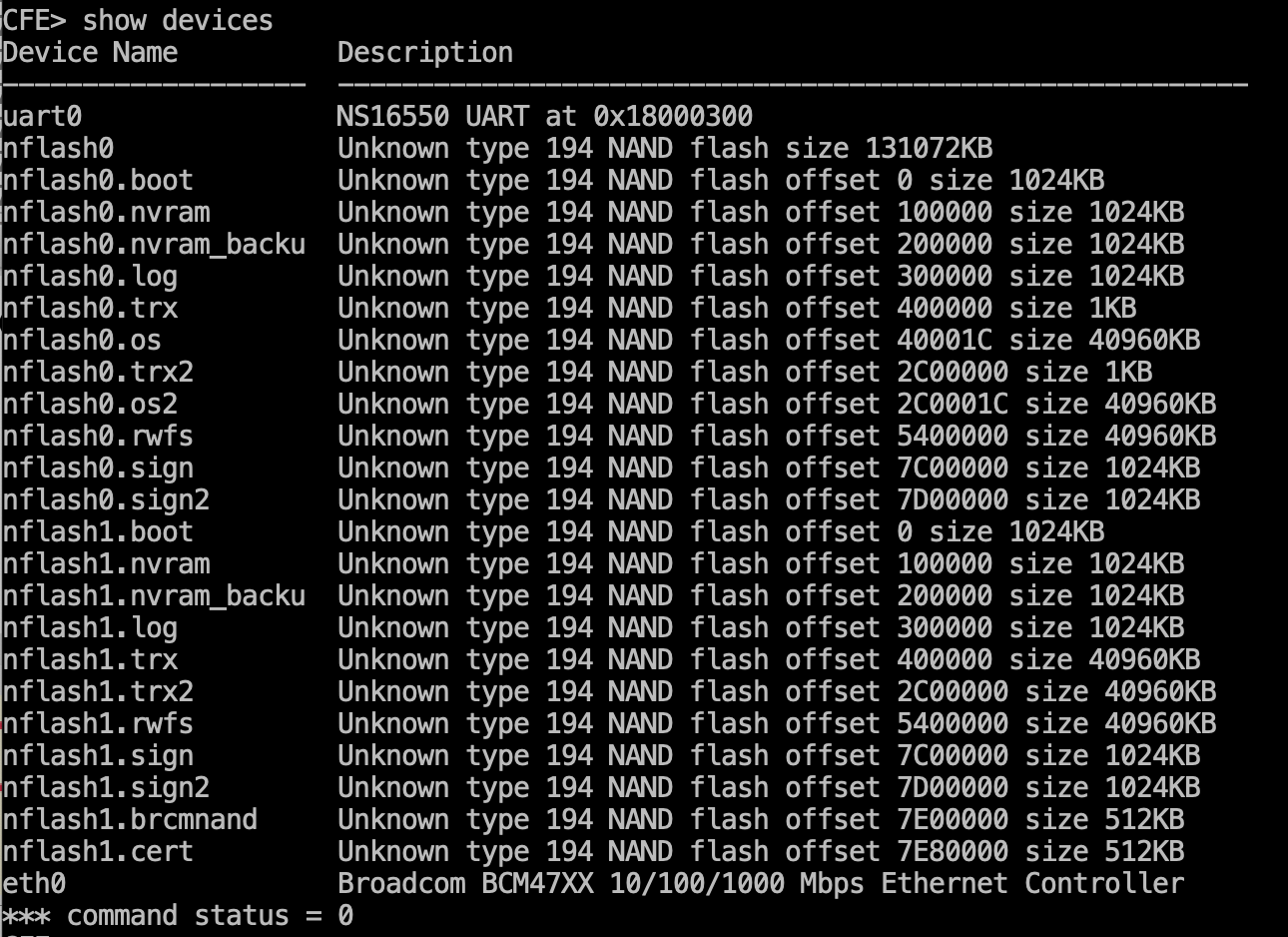
We are going to read 100 bytes from the nflash1.nvram device.

Now all we have to do is read the flash memory at address 0x40000.

Similarly, with U-Boot, it is possible to automate the memory reading process using PySerial.
Depending on the bootloader configuration, instead of spending time on firmware dumping via UART (sometimes it takes the whole night to download 15 MB), it is possible to send the data using the TFTP protocol or write information on a microSD.
…using JTAG interface
If you use JTAG, it is important to find out what equipment can interact with this interface. I am going to describe how to dump the firmware using the OpenOCD + Bus Pirate combination.

For that purpose, I will need OpenOCD software and a preset Bus Pirate configuration available in the Proxmark repository.
First, launch OpenOCD with this config.

Then connect Bus Pirate pins to JTAG Proxmark3 as follows: CS → TMS, MOSI → TDI, MISO → TDO, CLK → TCK, GND → GND, and 3.3 → 3.3.
Now it is time to connect to the launched service using port 4444 set in the config and enter a couple of commands.

Voila! We have found backup.bin file containing the firmware in the same directory.

The entire process took only 246 seconds, and we have the firmware!
…using I2C/SPI interfaces
These interfaces are primarily used on EEPROM (electrically erasable programmable read-only memory) chips. It is necessary to note that Arduino is not the best equipment for working with memory, but it still can be used.
At least two I2C/SPI firmware dump projects are available for Arduino: arduino-i2c-read-eeprom and spi-dump..
However, I do not recommend novice hackers to try these projects because the device can be fried easily if the pin connection is incorrect.

I would like to specially mention TL866Plus programmer able to work with EPROM, EEPROM, FLASH, SPI, I2C,93Cxx, ICSP, and other chips. It costs pennies in comparison with other similar devices.

The TL866Plus software is available only for Windows, but if you use another OS, it works well in the virtual environment. There are no problems with the device passthrough are expected. In addition, various sets of adapters are available for this programmer making it possible to connect it to different chips.

We are going to extract the firmware from JTAGulator without soldering – just using an SOP8 clip.

Important: during the work, JTAGulator was in the standby mode and powered via USB because the programmer could not supply enough power. To make sure that the device does not display any activity in the course of the firmware dumping, it is recommended to push and hold the Reset button on the chip.
First, I launch the software for TL866, Xpro. A screenshot of its interface is shown below.

The next photo shows the memory chip on the JTAGulator card; in my case, it is 24LC5121.

Selecting it in the program.

Then connecting the clip to the memory as shown on the picture.

Pressing the Chip Read button – and JTAGulator’s firmware is dumped.

Getting access to root console
If, for some reason, you cannot dump the firmware, you may try to get access to the admin’s control console using UART interface.
Boot arguments
Both the U-Boot and CFE boot loaders support functions allowing reading and setting global variables using printenv and setenvcommands.
First, let’s see what variables have been set by the developers.
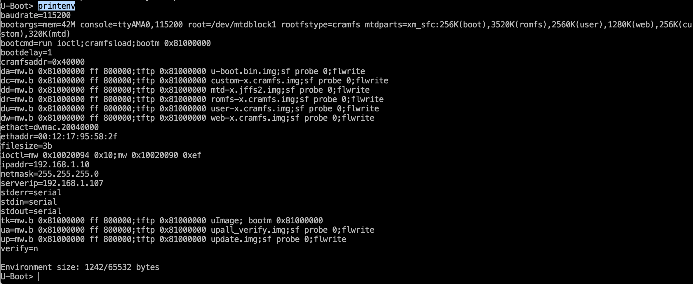
We are looking for the boot arguments variable, bootargs.
bootargs=mem=42M console=ttyAMA0,115200 root=/dev/mtdblock1rootfstype=cramfsmtdparts=xm\_sfc:256K(boot),3520K(romfs),2560K(user),1280K(web),256K(custom),320K(mtd)
To get the root access, we will try to add the path to Bash/BusyBox to the boot arguments in order to launch the root console automatically when the system starts. To do so, enter one of the following commands in the console:
$ setenv extra_boot_args init=/bin/sh
$ setenv optargs init=/bin/sh
$ setenv bootargs $ single init=/bin/sh
This method does not works very often. I would recommend watching the presentation of Synack at DEFCON 23: fourteen devices were tested, and for twelve of them, the root consoles have been accessed using this technique
Firmware reflashing
An Ethernet port is required to replace the device firmware using TFTP. It is necessary to enter the setenv command in the environment variables and set the network settings.
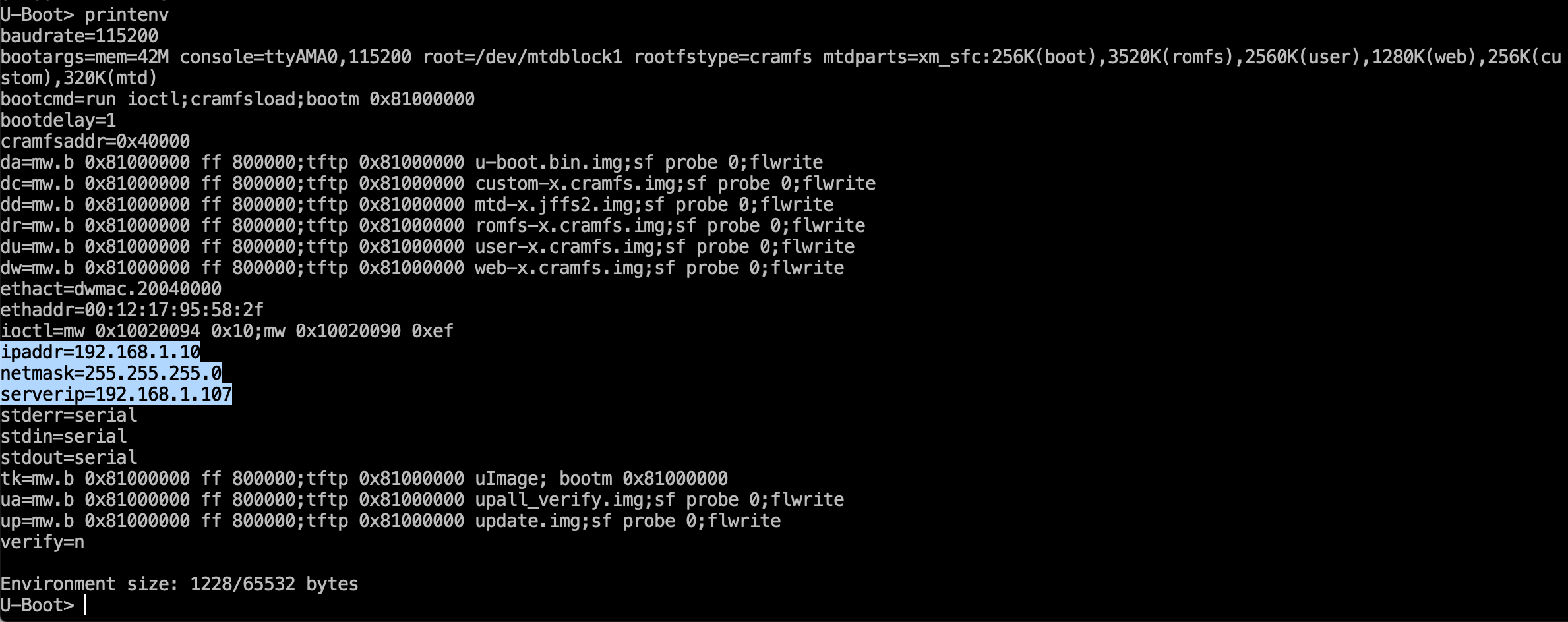
In our case, ipaddr is the IP address of the device, netmask is the network mask, while serverip is the address of the TFTP server on your computer. The tftpboot command syntax is as follows:
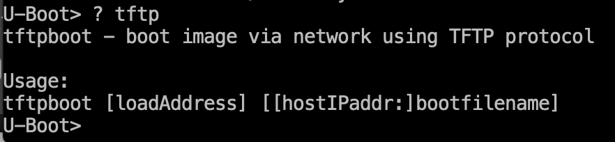
Now launch the TFTP server, place the firmware file into its folder, and load it into the device’s memory using the tftpbootcommand.
There is also another method: save the firmware onto an SD card and subsequently load it into the device’s memory using commands mmcinit and ext2ls.
Mmcinit initializes the SD card, while ext2ls loads the file from it into the flash memory. This procedure is described in detail in the OpenMoko Wiki.
Using the mw (memory write) command, you can write bytes directly to the flash memory. However, this process requires automation because, if the bytes have different values, the writing speed would be 4 bytes per one mw command cycle. The command syntax is as follows:

An example of the application of this command is shown below.

Sewing Needle method
This method is described in detail in a presentation delivered by pin2pwn at DEFCON 24, How to Root an Embedded Linux Box with a Sewing Needle.
The essence of this hack is to short together two of the data pins coming off the flash storage device that holds the kernel during the boot; this causes an exception in the startup script that takes us to the root console.

WARNING
Caution should be exercised while using this method because the device memory may be burned.
On that optimistic note, we are going to conclude the theoretical part. Now it is time for the practice. We have an exciting job to do: extract firmware from an IP camera.
Practical part: Extracting camera’s firmware
I used a WiFi Smart Camera in my experiment. This nice device resembles a hybrid of a hairdryer and a nightlight.

Because the camera was produced in China, it was not a problem to open it even without a screwdriver.

First, we are looking for the mainboard name.
The ‘reverse’ side.

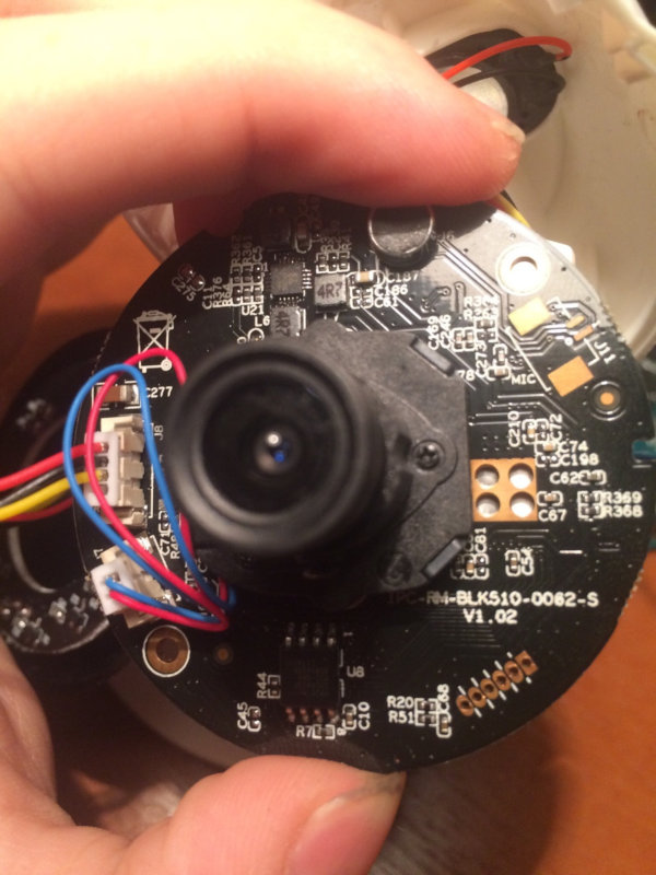
The name is shown on the first picture: IPG-RM-BLK510-0062-S. Let’s Google it.

Website 121.40.191.139:81 was inactive at the time of writing the article; therefore, I used Google cash.

The first column in the table provides contact pad labels on the board, the second one has socket numbers, the third and fourth columns store their names and functions.
Searching the table for ‘interesting’ interfaces, I find out that UART ports are located on J10 pad.

Now I have to locate it on the mainboard.

The number of pins matches that in the table, and they are numbered. Terrific! I connect Arduino to the following pins: GND (Ground), UART0_TXD (output) и UART0_RXD (input).
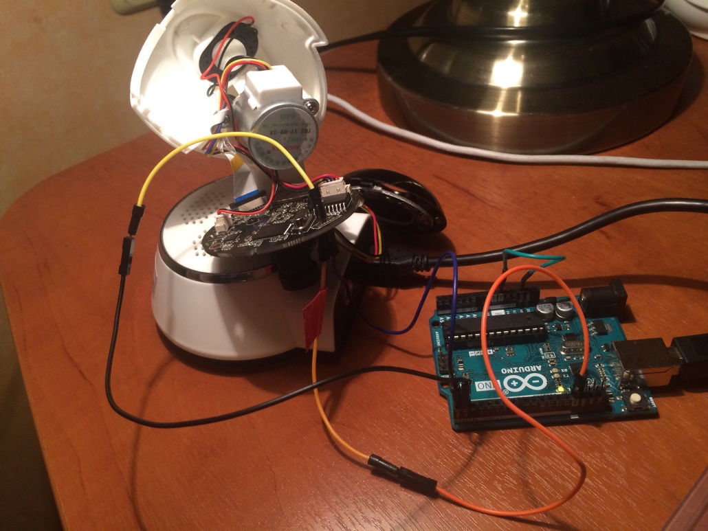
Then I launch a program for communication with serial devices; in my case, this is IO Ninja terminal emulator, network sniffer, and IO monitor. I restart the device and press Ctrl + C on the keyboard to launch the U-Boot console.
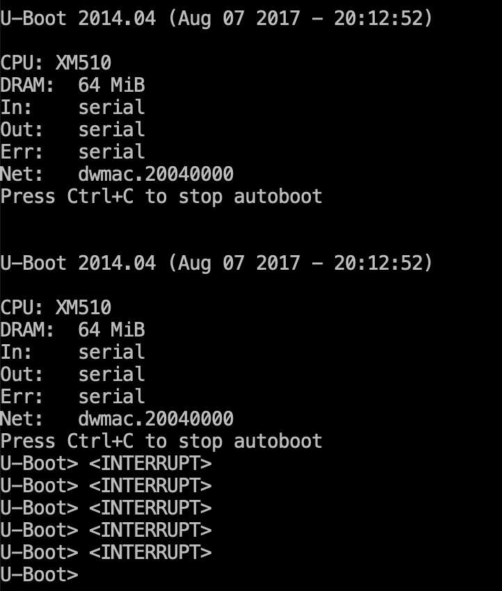
Alas, I failed to access the root console; so, proceeding to the next step. Use the commands cramfsls and cramfsload. Let’s try dumping the file with usernames and passwords.
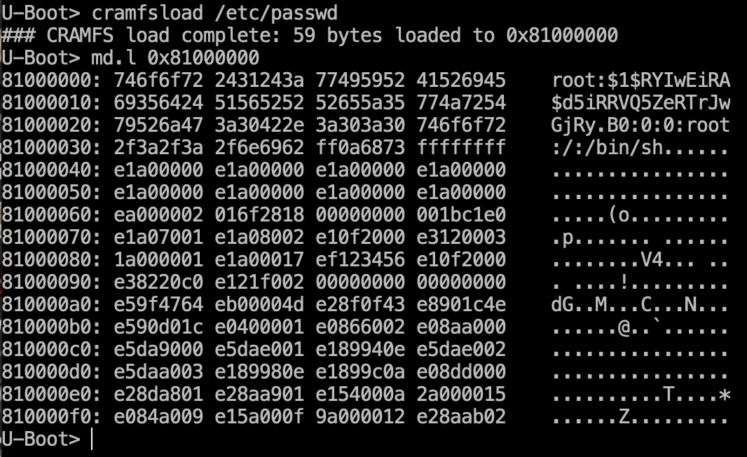
Yes! We have got the first password embedded in the camera:
root:\$1\$RYIwEiRA\$d5iRRVQ5ZeRTrJwGjRy.B0:0:0:root:/:/bin/sh
The decoded hash can be found on one of the forums.

So, the root password is xmhdipc. Now, let’s go back to the first photo of the mainboard.

The red box marks an EEPROM memory chip with an SOP8 connection pad. The name can be seen on it: 25L6433F. We Google it, find out that SPI interface is used to communicate with this chip, and locate its pinout scheme.
Too bad, I cannot read the chip memory directly from the mainboard. It has to be unsoldered and removed.

Connecting the removed chip to the programmer.

Saving the dump and soldering the chip back. Now I have to make sure that the file contains the information I need. To do so, I use Binwalk firmware analysis tool.

Let’s see what it managed to unpack.

All files have been retrieved from the device!
Conclusions
Our research into the hardware security of smart gadgets is complete. Of course, many aspects of this broad topic were not covered, while some of the sections require separate articles to address all possible situations. Still, I hope this reading will be helpful in your further inquests into the internal structure of smart gadgets around us.
Summer reading
- Security Engineering: A Guide to Building Dependable Distributed Systems – this book addresses in detail the physical security of devices;
- PentestHardware – notes of a tester of embedded systems; by its volume (150 pages) it is comparable with a book.
I love hardware hacking, and this is a great quickstart guide for all the folks I see asking if they can “do something with these weird pins on this thing I took apart”.. Some paraphrased version of that question is asked on the r/hardware_hacking thread at least once a week, and now I know where to send them!