We live in the world of digital electronic devices. Many TVs, car radios, monitors, routers, and computer/laptop motherboards store their control software in SPI Flash memory chips. Sometimes, to repair such devices or expand their functionality, you have to reflash them. In addition, such devices can be used to store small amounts of valuable information, which is extremely important for every hacker IT specialist.
A thing in itself
One day I encountered a SOHO Ethernet/Wi-Fi router that turned out to be a branded version of ZTE H118N. It was operational, but basically useless without a contract with an Internet provider. Settings in its web interface were blocked; network services were disabled; and Internet searches showed that the only way to turn it into something usable was to reflash its firmware (i.e. software stored in the permanent memory microcircuit). The manufacturer took certain precautions, and it was impossible to replace the contents of its read-only memory storage using the software method. But it was still possible to reflash the router with a programming device.
info
If you think that a screwdriver and a soldering iron grant you access to any electronic device, you are wrong. Some components of information systems used in the financial sector (e.g. payment terminals and ATMs) have physical protection in addition to software protection. If you attempt to open the case of such a device, the data stored in it can be irretrievably lost due to disconnection of the supporting power supply, or the storage media can be physically destroyed (e.g. by an electrical impulse from a prudently installed battery). In the latter case, you can even observe noise and smoke effects.
A brief research showed that some routers of this class support the Linux-based OpenWrt operating system that significantly expands their capabilities. Concurrently, I checked specialized forums and found out that an unsuccessful attempt to install this OS can ‘brick’ your router. In most severe cases, you have to load a ‘dump’ (firmware image) using a programming device. In addition, it turned out that routers from different manufacturers based on the same (or similar) hardware platform, can operate under the control of competitors’ software. Overall, everything encouraged me to perform bold experiments with the device I had.
What to do?
Too bad, my hope to create a compact universal Linux-based device has crashed into harsh reality. After removing its case cover, I discovered an RTL8676S microprocessor. There is very little technical information on it in the public domain, and the interest in it in the OpenWrt community is very low as well. Still, I decided to give this router a chance by replacing its firmware with the standard one used in similar devices.
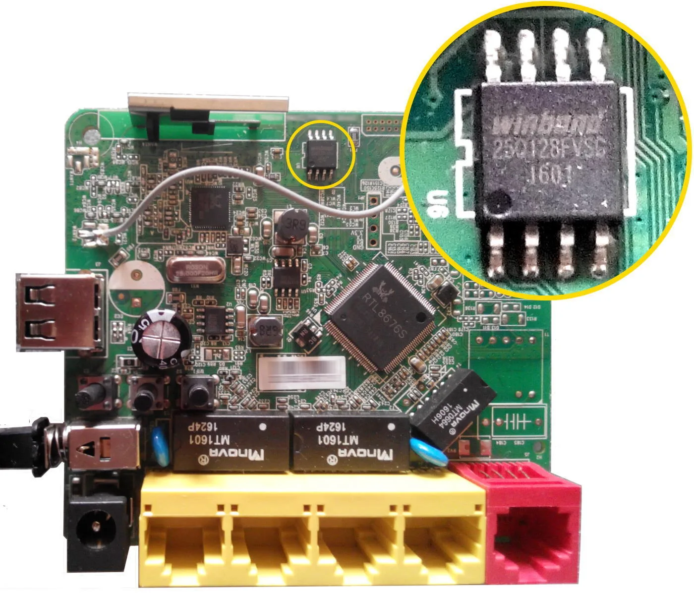
At the edge of the board, you can see an 8-pin W25Q128FVSG read-only memory chip that I’m going to reflash. According to the specification, its memory is based on the NOR Flash technology and can accessed via the SPI serial interface. The information capacity of this chip is 128 Mbit (16 MB), and it operates in the voltage range from 2.7 to 3.6 V.
www
The Winbond 25Q128FVSG specification is available on the manufacturer’s website.
Inexpensive USB programming devices based on the CH341A converter are widely used to program such ‘25-series microcircuits’. For in-circuit programming (the microcircuit isn’t removed from the board), it’s equipped with a special clamp-clip that grips the memory microcircuit and ensures the required contact. I didn’t have such a wonderful tool at hand, but I had an Arduino UNO clone. There is a frser-duino sketch for it that turns the device into a UNO programmer supporting the flashrom utility.
info
As you are likely aware, Arduino can be used to create user-friendly electronic components whose specifications are published under an open license. One of the most successful products is the UNO board: its ‘central’ ATMega328P microcontroller’ featuring the required support components and handy contact strips is equipped with the ATMega8U2 (versions R1 and R2) or ATMega16U2 (version R3) ‘co-controller’ implementing the USB—serial converter function, which simplifies loading programs to the device. By the way, software projects for Arduino and binary code compiled from them are called sketches.
Thanks to the open license and a large number of Arduino UNO fans, other manufacturers also produce similar devices with some modifications in the original scheme. For instance, to reduce the cost, USB—serial interfacing is often implemented using not a universal programmable ‘co-controller’, but a specialized CH340G interface chip.
To reprogram my experimental router, the following steps are required:
- Prepare working environment on a personal computer;
- Build the frser-duino sketch in the working environment using source texts;
- Write the frser-duino sketch to the Arduino UNO clone (i.e. transform it into an UNO programmer);
- Connect the SPI Flash chip to the UNO programmer; and
- Write the firmware from the image file to the SPI Flash chip.
Working environment
I used the Bodhi Linux 4.5 64 bit environment based on Ubuntu 16.04. Accordingly, the actions described below can be reproduced on all more or less modern Ubuntu-based Linux distributions. You only have to install the following packages:
- build-essential — tools required to build software from source texts;
- arduino-core — a metapackage containing the gcc-avr cross-compiler for AVR microcontrollers and the avrdude programming utility for them; and
- flashrom — a utility used to manage programming devices for memory chips.
To install the above-listed tools from the repository, use the command:
sudo apt install build-essential arduino-core flashrom
When you connect an Arduino clone board to a working computer using a USB cable, a serial port file / will be created:
crw-rw—- 1 root dialout 188,0 … /dev/ttyUSB0
To test its operation, enter the command:
avrdude -c arduino -p atmega328p -P /dev/ttyUSB0 -b 115200
It includes the following parameters: -c (specifies programmer type), lowercase -p (microcontroller model being programmed), uppercase -P (programmer serial port file), and -b (data exchange rate). The following information should appear on the screen:
avrdude: AVR device initialized and ready to accept instructionsReading
avrdude: Device signature = 0x1e950f (probably m328p)
avrdude: safemode: Fuses OK (E:00, H:00, L:00)
avrdude done. Thank you.
If, instead of it, you see the string
avrdude: ser_open(): can’t open device “/dev/ttyUSB0”: permission denied
this indicates that you don’t have access rights to the port. To gain them, you have to become a member of the dialout group and log in again:
sudo usermod -aG dialout hacker && exitOf course, your username should be entered instead of hacker. To check your group membership, use the groups command.
Did it work? Then, prior to moving on, make a backup copy of your Arduino clone’s flash memory containing the sketch and bootloader:
avrdude -c arduino -p atmega328p -P /dev/ttyUSB0 -U flash:r:uno_backup.hex:i
Several strings with information will be displayed on the screen again, and the file uno_backup. containing the flash memory image in Intel HEX format will appear in the current directory.
info
In the last command, I didn’t specify the baud rate parameter. By default, the avrdude program uses the 115200 value for Arduino-based programming devices. But if, for some reason, you see a series of ‘wrong baud rate’ messages, like this:
avrdude:
you can try to include this parameter into the command.
Building a sketch for a UNO programmer
To turn you Arduino clone into a UNO programming device, you have to write to it the machine code of the frser-duino sketch that has to be built from source texts. To get the source code from the Internet repository, use the following commands:
wget -O frser-duino.zip https://github.com/urjaman/frser-duino/archive/refs/heads/master.zip
wget -O libfrser.zip https://github.com/urjaman/libfrser/archive/refs/heads/master.zip
The next step is to unpack the source texts:
unzip frser-duino.zip
cd frser-duino
unzip ../libfrser.zip
rmdir libfrser
mv libfrser_master libfrser
From the frser-duino perspective, an Arduino UNO clone with the CH340G chip is an FTDI device; the only difference is that its maximum data exchange rate is not 2,000,000, but only 115,200 bps. Commands required to build the sketch are provided in the VISduino section of the README. file:
DFLAGS=-DFTDI make clean all
SERIAL_DEV=/dev/ttyUSB0 make program
The second command not only compiles the source code, but also immediately writes the resulting machine code to the device connected to the / port. Therefore, don’t forget to connect the Arduino clone to the USB port prior to executing this command. If you haven’t done this, you can flash the sketch from the frser-duino. file later using the command:
avrdude -c arduino -p m328p -P /dev/ttyUSB0 -b 115200 -U flash:w:frser-duino.hex
This command clears the contents of device’s flash memory, writes machine code to it, and runs a check. All operations are performed in a matter of seconds:
avrdude: Reading ..avrdude: ..avrdude: Writing ..avrdude: Reading ..avrdude: avrdude: avrdude
Wow! Do I really have a UNO programmer now? This can be checked using the flashrom utility:
flashrom -p serprog:dev=/dev/ttyUSB0:115200
Information about the utility, programming device, and memory chip will be displayed on the screen:
(1) flashrom v0.9.9-rc1-r1942 on Linux 4.4.262
(2) flashrom is free software, get the source code at https://flashrom.org
(3) Calibrating delay loop… OK.
(4) serprog: Programmer name is “frser-duino”
(5) serprog: requested mapping AT45CS1282 is incompatible: 0x1080000 bytes at 0xfef80000.
(6) No EEPROM/flash device found.
(7) Note: flashrom can never write if the flash chip isn’t found automatically.
If you see the name “frser-duino” in line 4, then congrats! Other messages can be ignored for now. Lines 6 and 7 say that memory for programming wasn’t found. This isn’t surprising since you haven’t yet connected an SPI Flash chip to the UNO programmer. The weird message about some incompatibility in line 5 can be disregarded: based on my experience, it doesn’t affect the quality of your UNO programmer.
But if you see the message:
…
Calibrating delay loop… OK
Error: cannot synchronize protocol – check communications and reset device?
Error: Programmer initialization failed
then, most likely, your Arduino clone is missing the frser-duino sketch (or it doesn’t work for some reason). Try to repeat the writing procedure. Hopefully, you’ll overcome this issue.
Connecting SPI Flash
To program this chip, you have to connect it to your UNO programmer. And this has to be done correctly, including two important aspects. First, the memory chip contacts must be connected to programmer’s pins used by its control software. Second, you have to ensure that the power levels, chip signals, and programmer signals match each other.
Connection diagram;
The first requirement can be fulfilled fairly easy. Just be careful and follow the diagram shown in the figure below. Pins 10–13 are reserved for the SPI bus. Their notations vary in different specifications, but you can use the following match between the Arduino, SPI bus, and SPI Flash chip notations:
- D10 — SS — SS — /CS — 1;
- D11 — COPI — MOSI — DI — 5;
- D12 — CIPO — MISO — DO — 2;
- D13 — SCK — SCK — CLK — 6.
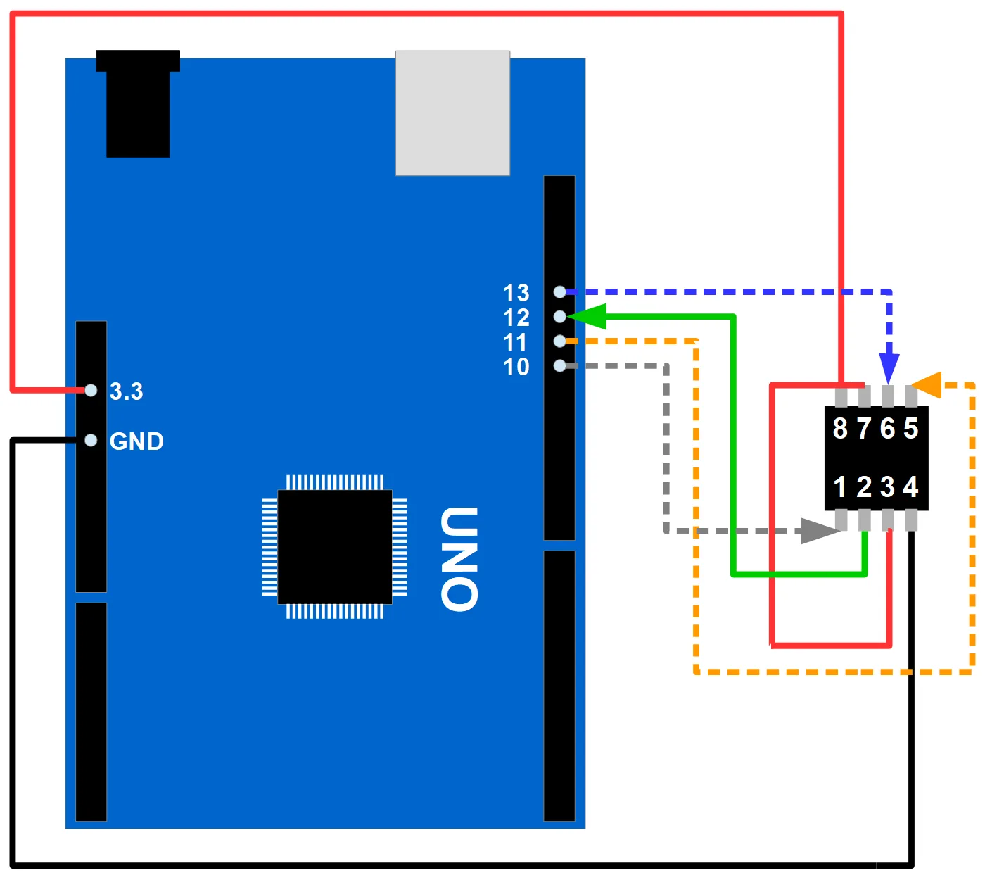
In addition, the SPI Flash chip must be included in the power supply circuit: the 3.3 V stabilizer output has to be connected to its 8th Vcc contact; while the common wire has to be connected to the 4th GND contact.
warning
On the UNO programmer side, the 5 V contact is located directly under the 3.3 V contact. Make sure that you don’t connect the chip to over-voltage!
Note that some SPI Flash chips have no visible differences from the one used in this experiment, but are designed for a voltage of 1.8 V. You cannot use them with this UNO programmer. Make sure to check the chip markings and parameters using manufacturer’s specification!
You might be surprised that the power line in the figure is connected not only to the 8th pin of the microcircuit, but also to its 3rd and 7th pins. Pin 3 (/WP — Write Protect) is designed to prevent modification of information stored in the memory chip. The slash in its notation indicates that it’s active low. When low voltage (logical zero) is applied to this pin, data can only be read from the chip. Such protection is a suitable solution for the BIOS microcircuit on a system board. But in this particular case, it has to be disabled by applying a high voltage level (logical one) to the pin.
Contact 4 (/HOLD) makes it possible to pause the memory chip for the time a low voltage level is applied to it (and this is again indicated by the slash in its notation). Since I don’t plan any pauses, a high voltage level is applied to it as well.
Voltage matching
As for the second requirement, you have no choice but to use your brain and a soldering iron. The presence of a 3.3 V power supply stabilizer in the UNO programmer doesn’t change the fact that it receives power from the USB connector and operates in 5-volt logic. According to the table in section 28.2 “DC Characteristics” of the ATmega328P microcontroller datasheet, the output voltage on the data lines can vary from 4.1 to 5 V. This means that a logical one will be transmitted along the data lines (shown by dotted lines in the diagram) using a voltage of some 5 V, which is too high for the memory chip.
warning
According to section 9 “Electrical characteristics” of the W25Q128FV chip datasheet, the Vcc supply voltage can reach 4.6 V; while the maximum voltage allowed on the Vio signal lines is Vcc + 0.4 V. In this case, Vcc = 3.3 V, and the absolute maximum for signals is 3.7 V, not 5 V.
On the Internet, you can find reports of successful operations with SPI Flash at over-voltage, but the manufacturer warns that this can result in product failure. If you have successfully crossed the street several times against a red light, this doesn’t mean that traffic lights aren’t required anymore.
As you probably remember from physics lessons at your school, voltage can be reduced using a divider consisting of two resistors (see below).
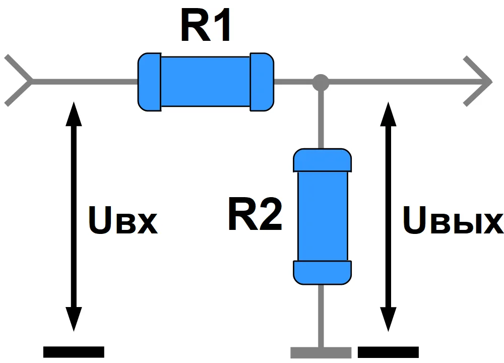
If the programmer output resistance is low compared to R1; while the memory chip input resistance is high compared to R2, then voltage at the divider output can be calculated as follows:
Uout = Uin * R2 / (R1 + R2)
From the “Electrical characteristics” sections of the ATmega328P microcontroller (the central element of a UNO programmer) datasheet and the W25Q128FV chip specification, you can find out the possible values of the low (logical 0) Vol and high (logical 1) Voh voltage levels at the microcontroller outputs, as well as permissible values of the low Vil and high Vih voltage levels at the memory chip inputs:
- Vol — from 0 to 0.8 V;
- Voh — from 4.1 V to Vcc;
- Vil — from –0.5 V to 0.3 Vcc; and
- Vih — from 0.6Vcc to Vcc + 0.5.
The supply voltage (Vcc) of the microcontroller is 5 V; while the supply voltage of the memory chip is 3.3 V as shown in the diagram below.

As can be seen, the low-level voltage falls within the permissible range; while the high-level voltage doesn’t.
www
Recommendations for matching voltage levels between a UNO programmer and a SPI Flash chip can be found on the flashrom website.
The voltage divider factor K = R2 / (R1 + R2) must ensure that both the upper and lower possible voltage limits at the microcontroller outputs fall within the permissible range. Let’s calculate the maximum and minimum values of thus factor:
- Kmax = 3.70 : 5.00 = 0.74; and
- Kmin = 2.31 : 4.10 = 0.56.
Now you can select resistors. The flashrom website suggests using R1 = 10 kOhm and R2 = 15 kOhm. The factor of such a divider is 15/25 = 0.6. Indeed, it meets the calculated requirements.
info
One might ask: why, instead of 10 kOhm and 15 kOhm, can’t you use resistors whose nominal values are, for example, a thousand times lower? After all, the factor of a divider based on such resistors is the same!
The answer is: you can’t because the total resistance of such a divider will be only 25 Ohm. According to Ohm’s law I = U / R, when a high voltage of 5 V appears at the microcontroller output, a current of 5 V / 25 Ohm = 200 mA will flow through the divider to the common conductor, which significantly exceeds the output line’s capacity, which is only 20 mA. If the high voltage level is maintained for long enough, the UNO programmer might go out of service.
Okay, but what if, instead of reducing the resistor ratings, you increase them a thousand times? First, it will no longer be possible to neglect the effect of the microcircuit input resistance on divider’s parameters; and second, the resistor R1 with a rating of 10 MOhm will limit the current to a value of 5 V / 10 MOhm = 0.5 μA, which won’t be sufficient for the microcircuit to detect the signal at its input. Such a high resistance can be considered a connection termination.
Practical implementation
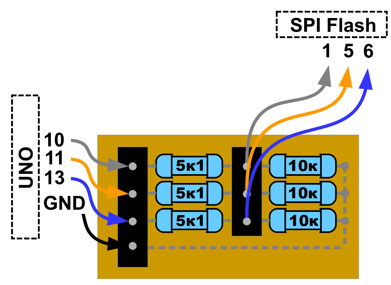
I didn’t have 15 kOhm resistors at hand, but I had plenty of 10 kOhm and 5.1 kOhm ones. If R1 = 5.1 kOhm and R2 = 10 kOhm, then the divider factor is 100/151 = 0.66. This is also an acceptable value, so I settled on this option. For ease of use, I assembled the circuit shown below on a breadboard.
warning
To avoid damaging the UNO programmer and SPI Flash chips, connect wires only when the programmer is disconnected from the USB power supply. Prior to turning it on, carefully inspect the assembled structure for correct connections and check it for the absence of accidental contacts between wires. The greatest danger is a short circuit between the VCC power line and the common GND wire.
Initially, I tried to solder wires to SPI Flash pins directly on the router board, and technically I succeeded. But the UNO programming device reported that it doesn’t see any chip:
No EEPROM/flash device found.
Perhaps, the power coming from the USB port wasn’t enough for this connection option. Since on-board programming failed, I decided to remove the chip from the board.
warning
Contact pads under the SPI Flash chip are sensitive to mechanical stress; if you try to remove the chip with a regular soldering iron, chances to damage them are very high. If you don’t have the appropriate experience and tools, it’s better to contact a specialized workshop to perform this operation.
Since I was planning multiple experiments with the test device, I had to somehow avoid constant impacts on the board. So, I connected a DIP8 socket to vacant contact pads using eight flexible wires some 5 cm long from a floppy drive cable. Then I installed the SPI Flash chip on the SOP8—DIP8 adapter board and soldered the connecting strips into its holes leaving the long ends of their plugs free. As a result, I got a ‘cartridge’ that can be repeatedly connected to the router board and disconnected from it.
To make programming more convenient, I assembled a special board for this cartridge to be able to connect it to the UNO programmer in the same simple way. The connecting wires of data lines are not shown in the figure below to avoid confusion. Just connect each colored circle to the square of the same color on the DIP8 socket with a jumper, and that’s it.
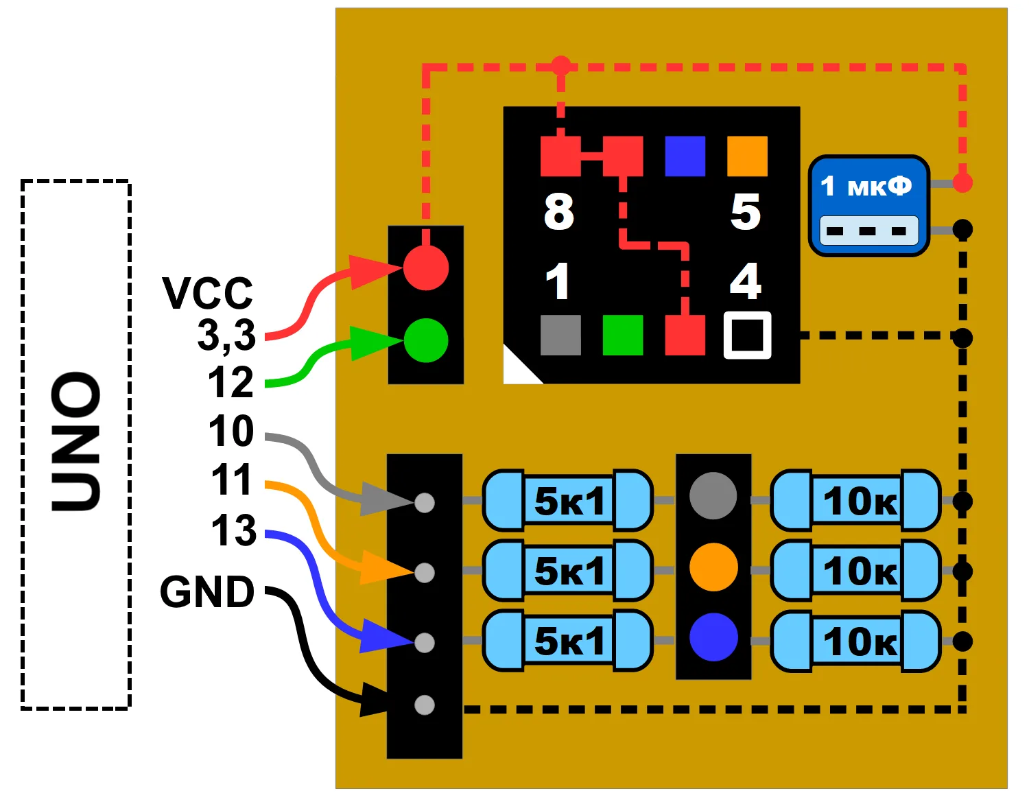
To avoid reconnection mistakes, I marked the corner of the chip near contact #1 and the corner with the respective slot connector on the board with white paint using a text corrector.
warning
Note that the electrolytic capacitor whose capacity is some 1 μF included in the power line requires the connection polarity to be observed.
Readiness test
To check the operation of the entire assembled system, you have to:
- correctly install the cartridge with the W25Q128FVSG chip on the SPI Flash board;
- correctly connect the UNO programmer to the SPI Flash board with flexible conductors; and
- connect the UNO programmer to the control computer with a USB cable and execute the command
flashrom -p serprog:dev=/dev/ttyUSB0:115200
If everything was done correctly, you’ll see the following response from the programming device:
flashrom v0.9.9-rc1-r1942 on Linux 4.4.262
…
Calibrating delay loop… OK.
serprog: Programmer name is “frser-duino”
serprog: requested mapping AT45CS1282 is incompatible: 0x1080000 bytes at 0xfef80000
Found Winbond flash chip “W25Q128.V” (16384 kB, SPI) on serprog.
No operations were specified.
The message “Programmer name is “frser-duino”” indicates that the flashrom utility was able to establish contact with the UNO programmer via USB; while the message “Found Winbond flash chip “W25Q128.V”” informs you that the UNO programmer has established contact with the SPI Flash chip via a set of conductors and identified its model. If the chip wasn’t identified, disconnect the UNO programmer from the computer and check whether it’s connected to the SPI Flash board correctly. You may see other messages, for instance:
Found Generic flash chip “unknown SPI chip RDID” (0 kb, SPI) on serprog.
or
Found unknown flash chip “SFDP-capatible chip” (16384 kB, SPI) on serprog.
Most probably, this indicates a poor contact somewhere in the connections between the UNO programmer and the SPI Flash board. Try to dress the wire tails; if necessary, bend them a little so that they fit tightly in the connectors. For signal lines, use wires no longer than 10 cm.
When you are 100% sure that everything works properly, read the contents of the SPI Flash chip twice and compare the resulting files dump1. and dump2.:
flashrom -p serprog:dev=/dev/ttyUSB0:115200 -c "W25Q128.V" -r dump1.bak
flashrom -p serprog:dev=/dev/ttyUSB0:115200 -c "W25Q128.V" -r dump2.bak
cmp dump1.bak dump2.bak && echo "No differences found."
Note that you have to specify the model of the memory chip whose contents you are reading in the -c parameter. Reading one dump takes some 24 minutes. During this procedure, the on and rx LEDs on the UNO programmer are constantly lit, and the tx LED blinks at intervals of some 2 seconds.
info
The bottleneck of this setup is the serial interface operating via USB connection between the control computer and the UNO programmer: the inexpensive CH340G chip used in the UNO programmer limits the reliable baud rate to 115,200 bit/s. The data transfer rate between the UNO programmer and the SPI Flash chip is much higher.
If instead of the phrase “No differences found” you see a message about differences in the dump files, then you have to find out the reason behind them. In most cases, differences occur due to poor contacts or too long connecting wires.
If no discrepancies were found, you can start programming the SPI Flash. But first you have to take one more important step.
Preparing firmware file
A firmware file represents an image of the contents of a memory chip. If these contents are read to a file, then everything is fine. But in the course of writing, it might turn out that the image is smaller than the memory capacity of the chip. In this particular case, the chip capacity is 16 MB; while the found file was read from a chip whose capacity is 8 MB. In such a situation, the UNO programmer behaves stupidly and ‘gives up’: in response to the command to write a dump from the file zte_h118n.
flashrom -p serprog:dev=/dev/ttyUSB0:115200 -c "W25Q128.V" -w zte_h118n.bin
the program responds:
Error: Image size (8388608 B) doesn’t match the flash chip’s size (16777216 B)
Therefore, you have to adjust the file size to the memory capacity. The easiest way is to add the missing FF bytes in the amount of 8 MB using the following command:
dd if=/dev/zero bs=8388608 count=1 | tr '\0' '\777' >> zte_h118n.bin
The dd utility takes the required number of values from the inexhaustible source of zeros (/), and the tr utility converts them into FF (\ is the octal notation for the hexadecimal number FF). After that, they are appended to the image file using the > command shell construct.
If the capacity of the new memory chip is a multiple of the old one’s capacity, it’s often recommended to use an image consisting of the respective number of duplicates of the original firmware. In this particular case, such an image, zte_h118n., can be easily created using the command:
cat zte_h118n.bin zte_h118n.bin > zte_h118n.new
Programming
Have you already connected the UNO programmer pins to the Flash memory board with the W25Q128FVSG ‘cartridge’ installed on it? Do you have the firmware image of the required size in the zte_h118n. file? If yes, connect the USB cable to the control computer and enter the command:
flashrom -p serprog:dev=/dev/ttyUSB0:115200 -c "W25Q128.V" -w zte_h118n.bin
The entire process takes approximately an hour and a half and involves the following operations:
- read the old contents of the memory;
- erase the memory and write new contents from the file
zte_h118n.; andbin - check the result of the writing operation.
You’ll see the following messages:
Found Winbond flash chip “W25Q128.V” (16384 kB, SPI) on serprog.
Reading old flash chip contents… done.
Erasing and writing flash chip… Erase/write done.
Verifying flash… VERIFIED.
After writing new data to the memory chip, I installed it into the router, turned it on… and nothing happened. I waited for a while, but indicators on its panel never lit up.
Conclusions
Even though the original firmware image written to the memory chip refused to operate on my equipment, let’s find out whether it was all in vain or not.
First of all, you’ve transformed an Arduino UNO clone into a useful device: an UNO programmer. Second, you calculated a resistor-based voltage divider and assembled an adapter board for safe operations with 3.3V SPI Flash chips. Third, you learned how to prepare a data image of the required size suitable for writing to SPI Flash chips. And finally, you used the UNO programmer to read data from a memory chip and write data to it. Overall, your knowledge, skills, and capabilities have increased significantly compared to the beginning of this journey.
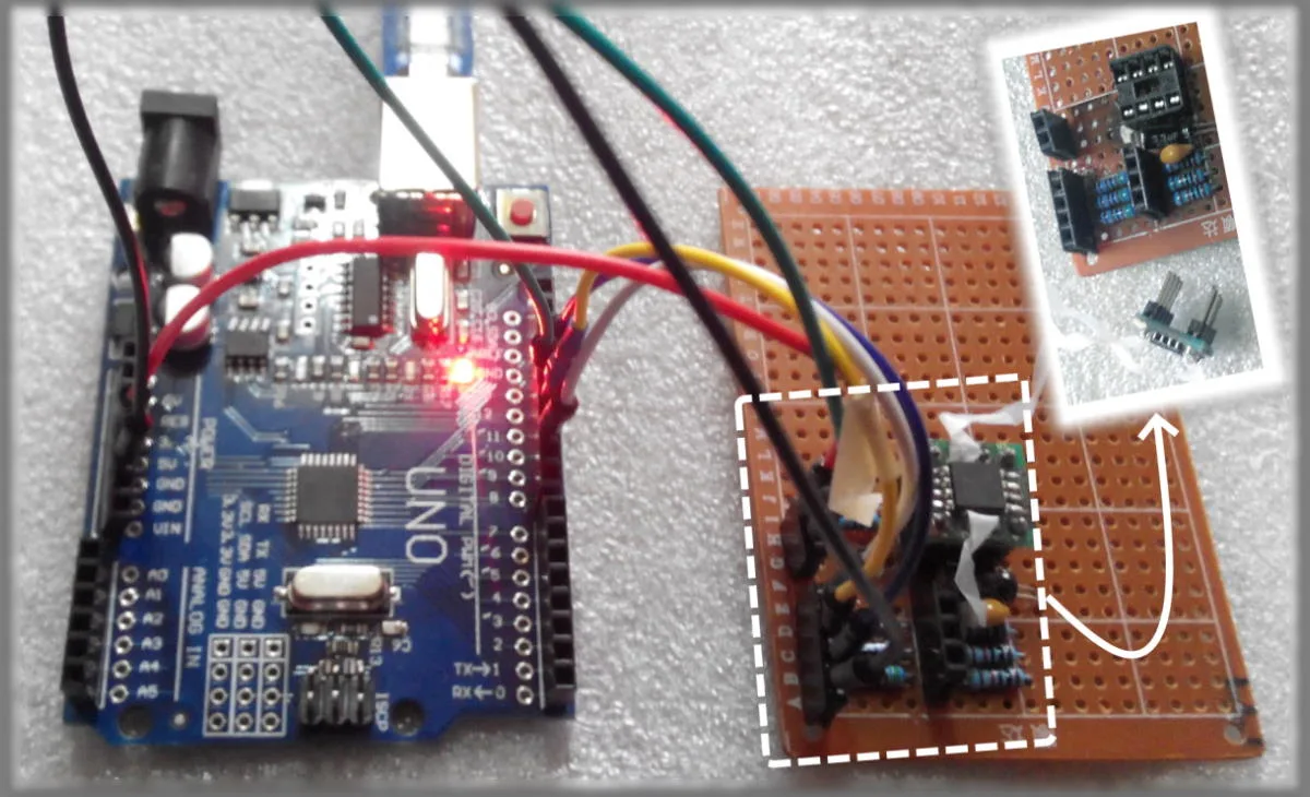
On top of everything else, SPI Flash chips are exciting devices in themselves. Their specifications state that they can withstand 100 thousand rewrite cycles, and data written to them can be stored for up to twenty years. Of course, the capacity of such chips is inferior to modern flash drives, and it takes a while to write data using an UNO programmer. However, their unusual form factor and nonstandard connection method can effectively protect your sensitive information from prying eyes. After all, you can write a ZIP archive to the chip instead of a firmware image…
And yet, the question is: What’s next? The name of the file containing the original dump indicates that it was extracted from a Macronix MX25L6406E chip. Its specification states that its electrical and geometric parameters are compatible with the already familiar Winbond 25Q128FVSG chip (only the memory capacity is two times smaller). Then why not try to write the firmware image to it? Who knows, maybe the router would ‘rise from the ashes’?
But this is a totally different story…
